Package Variants
1st level interconnects: FC or WB
Flip Chip Attach:
MR (SnAg or CuP w/ SOP or CuBOL w/o SOP) w/CUF or MUF
TCFC (TCNCP or TCNCF or TCCUF)
Substrate:
Singulated or strip
ETS or SAP
Package:
BGA, LGA, PGA, CSP, POP, QFN, WLP, SiP
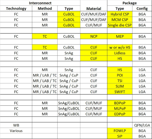
CSP Package Configurations
CUF: BD/HS/OM/OM-ED
MUF: OM/OM-ED
Package Evolution
WB->FC->WLFO->2.5/3D
WBPOP->FCPOP (BDP> MLP>EDP>MEP)->InFO
PoP Evolution
PoP is popular package configuration for smartphones, since this format allows integration of AP/baseband logic with DDR(DRAM) in limited space constraints (footprint & height) while maximizing performance (high speed & bandwidth for memory). Over time, has evolved from WB-POP to FC-POP, and now from BD-PoP to MLP-PoP.
Increasing performance requirements drives larger logic die and package body size, thin core or coreless/ETS substrates, all of which increase warpage that make meeting tightening coplanarity requirements, very challenging. Package height constraints further necessitate thin die/substrates that increase coplanarity/warpage concerns.
In addition, higher memory performance drives need for fine pitch memory, that require smaller ball sizes, which translates to smaller collapsed height or clearance between top & bottom packages.
MLP-PoP is an approach that (1) alleaviates above concerns of warpage & coplanarity, by making use of an overmold that adds structural robustness to the package and (2) enables fine pitch memory by improving the clearance between the 2 packages, without needing excessive die thinning.
This may be MLP-ED (exposed die) or MLP-OM (overmold). ED reduces overall package thickness but slightly higher cop/warpage is the resulting tradeoff. Further, this may be MLP-CUF v/s MLP-MUF
However, MLP-PoP requires additional molding processes - and comes at a premium (cost). Lower cost alternative is to use BD PoP with CuBOL for the bottom package, that increases package to package clearance by reducing die-to-substrate standoff.
Molded Embedded Packages
Molded Embedded Packages seek to overcome warpage concerns and limitations in z-height that conventional PoP type packages suffer from, where hybrid wirebonded/stacked die memories are stacked on FCBGA logic/ASIC SoC's, as commonly found in AP's of high-end flagship smartphones.
For MEP, first the active logic device is flip-chip attached on a base substrate. Then Cu Core balls are used to mount the top substrate on the base substrate with the interstitial space between the 2 substrates being encapsulated by a molding resin. Finally, BGA solder balls are mounted on the bottom substrate.
Since MEP does not require any gap between top and bottom packages as required in a conventional PoP (BD or MLP-ED/OM), by nature of the package construction, it allows for thinner PoP form factors. Landing pads routed to the top-side of the MEP allow DDR/DRAM memory to be mounted in a PoP format without any limitations from the layout of the (embedded) logic die (unlike conventional PoP's), enabling wide I/O memory interconnect with high bandwidth. This also allows using thinner memories reducing package z-height. Further, MEP packages have good warpage characteristics owing to similar material /structures between top & bottom substrates.
Inputs below from "Advanced Flip-Chip Package on Package Technology for Mobile Applications by Ming-Che Hsieh, Product & Technology Marketing, STATS ChipPac Pte. Ltd., Singapore".


TCNCP Process Profile
Tpre-heat -> Tstage ->Initial high speed approach upto search height -> Approach at search speed -> Contact (min force)-> Force ramp to max force (pressurization), bond head temp increased from stage (standby) temp to Tcontact -> temp ramp to Tpeak or Tcure ->cooldown and head disengagement.
Tbond-head(standby) = T stage -> to minimize any risk of NCP entrapment
Tbond-head(standby) = T contact -> for best throughput
Tbond-head(standby) > T contact -> risk of NCP entrapment
TCPNCP w/ OSP based finishes
TCNCP requires OSP surface finish (low cost, fine pitch process margins v/s Sn based finishes, controlled solder wetting v/s EPIG finish). However this requires use of fluxing agents in NCP material, to remove oxides during thermal compression bonding. Also it is critical to remove any residual OSP from the pad, since the OSP can combine with by-products of the fluxing reaction and lead to NCP entrapment. This therefore, requires an OSP pre-clean step, which comprises of plasma-treatment & chemical deflux, ahead of TCB.
CuPillar: Why, when & where
Mass reflow w/CUF (CuP) or Thermo compression bond (TCB/TCFC) -> TC-CUF, TC-NCP, TC-NCF
Electrical performance (current carrying capabilities, EM, fine pitch requirements) are driving CuP.
Mass reflow w/ Cu-pillar (CuP) maximizes UPH and therefore minimizes assembly cost. However, for large die packages, MR generates warpage concerns that can result in ELK/CPI issues. To counter this and lower package stresses, TCB or TCFC are process alternatives (but are low UPH options that end up increasing assembly cost/complexity):
TC-CUF: relatively lower cost alternative, but capillary UF flow may need vacuum underfill or pressure curing
TC-NCP: relatively medium cost alternative
TC-NCF: highest cost, application limited to thin die/ smaller FF packages/ ultra fine pitch
Shrinking pitch & die size: MR + Pb-free solder, MR + CuP/CuBOL, TC-CUF, TCNCP, TCNCF
An Acronymously Brief History of Semiconductor Packaging
CERDIP -> PDIP -> SOP/QFP -> BGA & FCA -> QFN -> CSP/WLP -> PoP/SiP -> SoC -> TSV/TSI
SoC Components:
Some digital logic (CPU, GPU & chipset logic such as GNB); Memory (DDR RAM, cache); analog signal & power management (sensors, drivers, actuators, controllers), interconnect buses & interfaces (PCI, HT) and DfT structures (BIST, JTAG Boundary Scans)
I am grateful for this blog to distribute knowledge about this significant topic. Here I found different segments and now I am going to use these new instructions with new enthusiasm.
ReplyDeletePneumatic Bottle Cappers